Project Description
Main Project Image
The project owner hasn't added main project image yet.
Project description
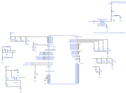
Bluetooth Dual Mode Module Design
- Dual mode [works for booth Bluetooth Low Energy and Bluetooth 4.0 (legacy) communication protocols]
- Based on Texas Instruments bluetooth chip CC2564
- Schematics based on the design reference from Texas Instruments CC2564
PCB considerations:
- 4 layer board
1st - top layer = signal layer, crystal oscillators, decoupling power capacitors, and chip antenna
2nd - Ground plane
3rd - Power plane
4th - bottom layer = signal layer
PS: The decision to place these components (crystal oscillators, decoupling capacitors, and the chip antenna ) on the top layer was made because the traces for these components should be the shortest possible in order to avoid signal or power traces noise. Recommendations from the reference design given by Texas Instruments.
- 10 mils trace width for power and antenna traces;
- 5 mils for all other traces;
- 3 mils minimum clearance for copper to copper;
- Via with 18 mils of size and 8 mils for hole;
- All vias below components have solder mask to prevent short circuit when reflowing/soldering SMD components;
- Designed to be as small as possible, can be modified for a bigger board with 2 layer;
- CC2564 footprint based on Texas Instruments reference design and documentation;
Antenna considerations:
- Be aware that the performance of the chip antenna (shown in the datasheet) was measured using a specific ground plane size and shape; in other words, the ground plane total area and shape modifies the antenna performance. Therefore, after integrating this PCB to your own design, consider building a prototype to test the antenna performance.
- It is important to keep the size of the antenna keepout and the feed point positioning/distance, please check the chip antenna datasheet.
- Alternatively, you can change the chip antenna to whatever you want/need (for instance - PCB pattern antenna or dipole antenna), just remember to match the impedances from the chip pins to the antenna, that usually is 50ohms
MODULE Pins description:
- 1- VDD_1V8 - Input - Power Supply (1.8V nominal)
- 2 - VBAT_CC - Connect directly to battery (range 2.2V - 4.8V).
- 3 - SHUTDOWNn_1V8 - Input - Shutdown input (active low). For more information see page 10 of the datasheet.
- 4 - GND - Ground (0V).
- 5 - AUD_CLK_1V8 - I/O - Pulse code modulation (PCM) clock.
- 6 - AUD_FSYNC_1V8 - I/O - PCM frame-sync signal.
- 7 - AUD_IN_1V8 - Input - PCM data input.
- 8 - AUD_OUT_1V8 - Output - PCM data output.
(Host Controller Interface - HCI)
- 9 - HCI_CTS - Input - HCI UART clear-to-send. The CC2564 device is allowed to send data when HCI_CTS is low.
- 10 - HCI_RTS - Output - HCI UART request-to-send. The host is allowed to send data when HCI_RTS is low.
- 11 - HCI_RX - Input - HCI universal asynchronous receiver/transmitter (UART) data receive.
- 12 - HCI_TX - Output - HCI UART data transmit.
- 13 - TX_DEBUG_1V8 - Output - TI internal debug messages. TI recommends leaving an internal test point.0.0
Technical documents/information about the CC2564: http://www.ti.com/product/CC2564/technicaldocuments
Gallery
The project owner hasn't added any images yet.
Design Files
Embed Code
Component (24)
Qty
Description
Capacitor
C15, C3
2
Generic Capacitor (0.1uF)
Inductor
L2
1
Generic Inductor (2.7nH)
Capacitor
C5
1
Generic Capacitor (0.47uF)
Capacitor
C12
1
Generic Capacitor (12pF)
Show More
Show Less
Export Design Data
Show More
Show Less
Comments
