Project Description
Main Project Image
The project owner hasn't added main project image yet.
Project description
Radio Frequency (RF) Transceiver
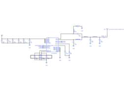
- Based on Texas Instruments chip CC110L;
- Receive and Transmit capabilities (64-Byte RX and TX FIFO);
- Tuned to work at 433MHz, but can be changed to other frequency bands (from 300 to 928MHz), please refer to datasheet for detailed information;
- 2-FSK, 4-FSK, GFSK, MSK, and OOK Supported;
- Schematics and PCB layout based on the design reference from TI CC110L;
- The crystal oscillator capacitors were calculated using the datasheet as reference (Load capacitance = 8pF);
PCB considerations:
- 2 layers board;
- 10 mils trace width for power;
- 16 mils trace for antenna;
- 6 mils for all other traces;
- 6 mils minimum clearance for copper to copper;
- Via with 13 mils hole and 7 mils annular ring;
- All vias below components have solder mask to prevent short circuit when reflowing/soldering SMD components;
- CC110L footprint based on Texas Instruments reference design and documentation;
Antenna considerations:
- Be aware that the ground plane total area and shape modifies the antenna performance. Therefore, after integrating this PCB to your own design, consider building a prototype to evaluate the antenna performance.
- It is important to keep the size of the antenna keepout (please refer to the datasheet for more information);
- Alternatively, you can change the antenna to whatever you want/need (for instance - PCB pattern antenna or dipole antenna), just remember to match the impedances from the chip pins to the antenna, that usually is 50ohms
MODULE Pins description:
- 1 - VDD - Power supply input (1.8V - 3.6V).
- 2 - GND (0V).
Digital I/Os:
- 3 - GDO0 - Digital I/O - Digital output pin for general use:
•Test signals •FIFO status signals •Clear channel indicator
•Clock output, down-divided from XOSC •Serial output RX data •Serial input TX data
- 5 - GDO2 - Digital OUT - Digital output pin for general use:
•Test signals •FIFO status signals •Clear channel indicator
•Clock output, down-divided from XOSC •Serial output RX data
Serial Interface:
4 - SO/GDO1(MISO) - Digital OUT - Serial configuration interface, data output ; optional general output pin when CSn is high;
6 - SI(MOSI) - Digital IN - Serial configuration interface, data input;
7 - SCLK - Digital IN - Serial configuration interface, clock input;
8 - CSn(SS) - Digital IN - Serial configuration interface, chip select (please refer to datasheet for detailed information);
Technical documents/information about the CC110L:
- http://datasheet.octopart.com/CC110LRGPR-Texas-Instruments-datasheet-26769718.pdf
- http://www.ti.com/tool/CC110LEM-433-RD#Technical Documents
Gallery
The project owner hasn't added any images yet.
Design Files
Embed Code
Component (22)
Qty
Description
Capacitor
C12
1
Generic Capacitor (220pF)
Capacitor
C15, C16
2
Generic Capacitor (0.1uF)
Capacitor
C1
1
Generic Capacitor (0.1uF)
Capacitor
C8
1
Generic Capacitor (3.9pF)
