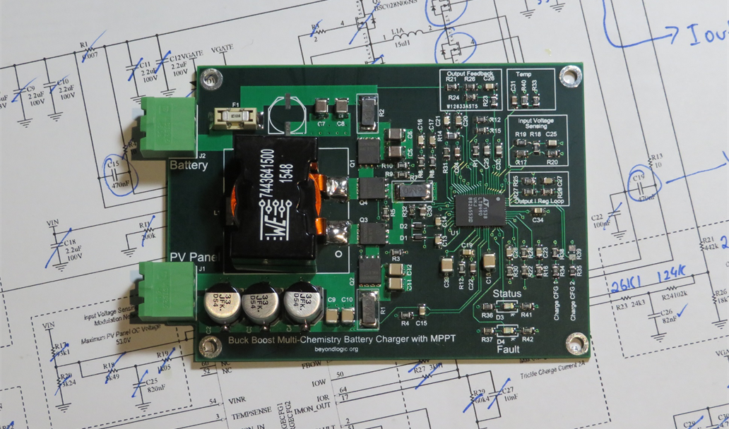
Buck-Boost Multi-Chemistry Battery Charger with MPPT

Project Description
Project description
This design is based on a Linear LT8490 High Voltage, High Current Buck-Boost Battery Charge Controller with Maximum Power Point Tracking (MPPT).
Most PV solar regulators are buck regulators and require the PV panel voltage to be above the battery voltage. This design uses a buck-boost topology and allows the PV solar voltage to be above, below or equal to the battery voltage.
The IC itself allows for a PV panel voltage in the range of 6V to 80V. Please note this design uses 63V input capacitors, and these would need to be switched out for panel voltages exceeding approximately 50V. The low voltage shutdown is configured for 5V.
The LT8490 will charge both Lead Acid and Lithium Batteries between 1.3V and 80V. Again, please observe output capacitor voltage ratings – The output caps in this design are rated at 35V but can be replaced with higher voltage ratings, if required.
The MPPT (Perturb and Observe) and charging algorithms are incorporated into the LT8490 - hence no programing is required.
Setup
This design can be heavily customisable to different battery chemistries, voltages and charging currents, in addition to various input power sources (i.e PV Solar Panels, Plug Packs etc). This customisation is made predominately through resistor changes, but may also require changes to MOSFETs and Inductors.
The battery chemistry and the number of charging stages can be set up by resistive divider networks on CHARGECFG1 and CHARGECFG2 pins. Maximum bulk and trickle charging rates can be set with resistor changes in the Output Current Regulation Loop.
Resistor values used are generally selected from the 1%, E96 range.
Input Voltage Sensing and Modulation Network
PV Solar panels are commonly manufactured in 36 and 72 cell arrays. Each cell produces approximately 0.5 volts and hence panels will typically have either an 18 volt or 36 volt output at PMAX, and an even higher open circuit voltage.
While the LT8490 utilises a MPPT Perturb and Observe algorithm, some set-up is required to the input voltage sensing and modulation network to select the maximum panel voltage. Arbitrarily setting VMAX to 80V may not result in the best operation of the LT8490 for all conditions, particularly at low input voltages.
The following table provides some common values for the input voltage sensing and modulation network:
|
VMAX |
RFBIN (kΩ) |
RFBIN2 (kΩ) |
RDACI1 (kΩ) |
RDACI2 (kΩ) |
CDACI (nF) |
|
R17 |
R20 |
R19 |
R18 |
C25 |
|
|
23.2 |
95.3k |
7.32k |
15.4k |
2.94k |
330nF |
|
53.0 |
93.1k |
3.24k |
1.05k |
5.49k |
82nF |
Notes:
- If powering the circuit from a DC Supply, the VINR voltage divider network should be pulled low. Remove R22.
Input Current Limiting
The maximum input current limit should be set at approximately 120 to 130 percent of the maximum current capability of the PV panel. The LT8490 will digitise the current reading (via the IIR/Current Input Read pin) and use this for the MPPT algorithm. Setting this value higher than necessary may reduce the accuracy of the MPPT calculations.

The maximum input current limit is set by the input sense shunt RSENSE1 (R1) and is converted to a voltage using RIMON_IN (R30). The datasheet recommends to use 21kΩ for RIMON_IN, hence:
RSENSE1 = 0.0505 / IN(MAX)
|
RSENSE1 (R1) (Ω) |
RIMON_IN (R30) (Ω) |
IIN(MAX) (Amps) |
IIN(MAX w/MARGIN) |
|
0.004 |
21k |
12.6 |
< 9.7 |
|
0.005 |
21k |
10.1 |
< 7.8 |
|
0.006 |
21k |
8.4 |
< 6.5 |
|
0.007 |
21k |
7.2 |
< 5.5 |
|
0.008 |
21k |
6.3 |
< 4.9 |
|
0.009 |
21k |
5.6 |
< 4.3 |
|
0.010 |
21k |
5.1 |
< 3.9 |
CIMON_IN reduces ripple and helps to stabilise the input current limit control loop. According to the datasheet, a value of 4.7nF to 22nF is deemed adequate for most applications.
Minimum Operating Voltage
The minimum operating voltage to enable the switching regulator is set via the R12/R15 voltage divider. The default setting in this design is 5V, the minimum operating voltage of the LT8490.
Charging Stages
The battery charger has the flexibility to cater for up to four different charging stages to suit both Lead Acid and Lithium battery chemistries.
Stage 0 provides a trickle charge for batteries that have a terminal voltage between 35 and 70% of the stage two voltage limit. This stage is designed to safely charge significantly depleted batteries and is configured by the Output Current Regulation Loop.
Stage 1 provides a full constant current output. This is also configured by the Output Current Regulation Loop.
Stage 2 provides a constant voltage charge when the battery reaches approximately 98% of the stage 2 voltage limit. All voltages are referenced to the Stage 2 voltage limit and this voltage is configured by the Output Feedback Resistor Network.
Stage 3 is optional and charges the battery with a reduced voltage configured by the CHARGECFG1 pin. This stage is most commonly used as a ‘float’ stage with lead acid batteries. It is entered from stage 2 when the charging current drops below C/10.
Charge Current Limiting
The maximum charging current is set by the output sense shunt resistor RSENSE2 (R2) and converted to a voltage using RIMON_OUT (R29). It is read via the IOR (Current Output Read) pin.

The IOW output is used to enable the Stage 1 Trickle Charging Current.
RSENSE2 = 0.0497 / IOUT(MAX)
|
RSENSE2 (Ω) |
RIMON_OUT (Ω) |
RIOW (Ω) |
RIOR (Ω) |
IOUT(MAX) (A) |
IOUT(MAXSO) (A) |
|
R2 |
R29 |
R25 |
R27 |
||
|
0.01 |
60.4k |
40.2k |
3.01k |
4.97 |
2.00 |
CIMON_OUT reduces ripple and helps to stabilise the output current limit control loop. According to the datasheet, a value of 4.7nF to 22nF is deemed adequate for most applications.
Output Feedback Resistor Network
The Output Feedback Resistor Network sets up the Stage 2 Voltage limit (VS2) - the maximum battery charging voltage. All other stage voltages are referenced to this voltage.
The following table provides some common values for the output feedback resistor network:
|
Battery Voltage |
Target VS2 (V) |
RFBOUT1 (kΩ) |
RFBOUT2 (kΩ) |
RDAC01 (kΩ) |
RDAC02 (kΩ) |
CDACO (kΩ) |
|
R21 |
R26 |
R23 |
R24 |
C26 |
||
|
12V SLA |
14.2 |
274 |
23.2 |
26.1 |
124 |
82 |
|
24V SLA |
28.4 |
487 |
20 |
28 |
107 |
68 |
|
48V SLA |
56.8 |
1000 |
20 |
22.6 |
115 |
100 |
CHARGECFG1 and CHARGECFG2 Setup
Status and Fault Indicators
The charger includes two LEDs to indicate the Charging Status or the presence of a Fault condition.
The following table indicates the Charging Status:
|
Charger Status |
Number LED Pulses, Flash Duration |
Name |
|
|
Status LED |
Fault LED |
||
|
Stage 0 |
1, 10ms |
OFF |
Trickle Charge |
|
Stage 1 |
1, 250ms |
OFF |
Constant Current (CC) |
|
Stage 2 |
2, 250ms |
OFF |
Constant Voltage (CV) |
|
Stage 3 |
3, 250ms |
OFF |
Reduced Constant Voltage (Optional) |
The Fault LED will provide a number of pulses (1-4) to indicate a fault according to the following table:
|
Charger Status |
Number LED Pulses, Flash Duration |
|
|
Status LED * |
Fault LED |
|
|
Battery Present Detection Fault |
1, 10ms |
1, 250ms |
|
Invalid Battery Temperature Fault |
1, 10ms |
2, 250ms |
|
Timer Expiration Fault |
1, 10ms |
3, 250ms |
|
Battery Under-voltage Fault |
1, 10ms |
4, 250ms |
* The Status LED can double as a UART providing feedback to an external device, hence the reason for the 10mS flash.
Enclosure
The PCB has been designed to fit into a Hammond 1591SFLBK Enclosure with 1591F Flange.
Release Notes
|
1.A.3 |
2nd November 2016 |
Prototype board sent to manufacture. |
|
|
15th November 2016 |
Fixed problem with bootstrap caps (D1/D2/C13/C14) wiring. Tidy up designator for R11. |
|
|
8th January 2017 |
Swapped CSPIN/CSNIN to fix Input Current Regulation Loop. |
|
|
14th January 2017 |
Fixed up footprint for C1 (EEEFK1H151P). Footprint was too small. |
|
1.A.5 |
14th January 2017 |
Production Release - V1.0 |
|
|
17th January 2017 |
Added J3 to disable MPPT (Enable Charging from DC Power Source) |
Gallery
External Links
Design Files

Embed Code
High Voltage, High Current Buck-Boost Battery Charge Controller with Maximum Power Point Tracking (MPPT), 6 to 80V, -40 to 125 degC, 58-Pin QFN(UKJ64)
U1
POWER_OBJECT
LTST-C170KRKT
D3, D4
08055C104JAT2A
C24, C22, C31