Solar Power Charger 2A Lithium SLA

Project Description

Project description
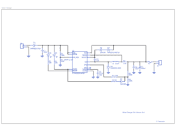
This project is based on a Linear Technology LT3652 Power Tracking 2A Battery Charger for Solar Power.
Featuring a wide 5 to 32V input range and input supply regulation loop for peak power tracking, this battery charger suits Li-Ion/Li-Polymer, LiFePO4 and SLA chemistries with a programmable maximum battery voltage of 14.4V and a maximum current of 2 amps.
The current schematic design is for a 2A, 12V SLA (Sealed Lead Acid) charger with 13.8V float voltage after C/10 has been reached.
The R1/R2 voltage divider sets the maximum power point voltage to 17.2V. The maximum charging current is reduced when the input voltage is below 17.2V (VIN_REG pin is under 2.7V). Set this voltage divider to your PV Panel’s VMPP (Voltage at Maximum Power Point).
The maximum charging current is set by R3. A 0.05 ohm shunt sets the maximum charging current at 2A, the maximum current possible from the LT3652.
The R6/R8 voltage divider sets a battery voltage of 14.4V. R6/R8 should be selected to obtain a 3.3V input on the VFB pin. This feedback pin has an 110nA input bias and can be compensated using a voltage divider with a 250k equivalent resistance. R7 is calculated to compensate the network and obtain this 250k equivalent resistance.
R9/D7 are optional and can be used with Sealed Lead Acid batteries to set a float voltage after C/10 has been reached. i.e. for a 12V SLA battery, the initial battery voltage can be selected to be 14.4V, and this reduces to a float voltage of 13.8V once C/10 is reached and the CHRG LED is extinguished.
The boost pin is used to bootstrap the internal switch gate. It has an operational range of 0 to 8.5V. As such, 6.2V Zener D3 is used to reduce the potential on the boost pin.
Use the following table to adapt the design for other battery chemistries:
| Battery Chemistry/Cells |
Charge Voltage |
R6 | R7 | R8 |
|---|---|---|---|---|
| 12V SLA | 14.4 | 309k | 174k | 100k |
| 1S LiPo (3.7V) | 4.2 | 27.4k | 226k | 100k |
| 2S LiPo (7.4V) | 8.4 | 154k | 191k | 100k |
| 3S LiPo (11.1V) | 12.6 | 280k | 174k | 100k |
Release Notes
|
1.A.3 |
18th May 2017 |
Prototype board sent to manufacture. Tested with 12V SLA - Functions as intended. |
|
1.A.4 |
10th June 2017 |
Resolved issue with bottom pads on J1 & J2 that had soldermask applied (i.e. were completely tented on bottom) preventing soldering. |
Observations
The LT3652 incorporates a thermal foldback protection feature that throttles the charging current back as the junction temperature approaches 125 degrees centigrade. While the exposed pad of the IC is connected the bottom of the PCB, the small board size of just 34 x 41 mm means the package has trouble dissipating enough heat when the charging current exceeds 1.5A at room temperature. In this environment, when setting a charging current of 2A the device will throttle back to about 1.5A. Attaching a heatsink to the underside of the board returns the charging current to just under 2A.
Gallery
External Links
Design Files
Embed Code
LT3652EDD#PBF
U1
7447779122
L1
MCS1632R050FER
R3
1N4148WS
D2, D7