Spice Library
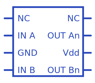
.SUBCKT TC4423A_I2D_B 1 2 3 4
* | | | |
* | | | Negative Supply
* | | Positive Supply
* | Output
* Input
*
********************************************************************************
* Software License Agreement *
* *
* The software supplied herewith by Microchip Technology Incorporated (the *
* 'Company') is intended and supplied to you, the Company's customer, for use *
* soley and exclusively on Microchip products. *
* *
* The software is owned by the Company and/or its supplier, and is protected *
* under applicable copyright laws. All rights are reserved. Any use in *
* violation of the foregoing restrictions may subject the user to criminal *
* sanctions under applicable laws, as well as to civil liability for the *
* breach of the terms and conditions of this license. *
* *
* THIS SOFTWARE IS PROVIDED IN AN 'AS IS' CONDITION. NO WARRANTIES, WHETHER *
* EXPRESS, IMPLIED OR STATUTORY, INCLUDING, BUT NOT LIMITED TO, IMPLIED *
* WARRANTIES OF MERCHANTABILITY AND FITNESS FOR A PARTICULAR PURPOSE APPLY TO *
* THIS SOFTWARE. THE COMPANY SHALL NOT, IN ANY CIRCUMSTANCES, BE LIABLE FOR *
* SPECIAL, INCIDENTAL OR CONSEQUENTIAL DAMAGES, FOR ANY REASON WHATSOEVER. *
********************************************************************************
*
* The following MOSFET drivers are covered by this model:
* 3A Inverting Driver - TC4423A
*
* Polarity: Inverting
*
* Date of model creation: 11/14/2008
* Level of Model Creator: G
*
* Revision History:
* 11/14/08 RAW Initial model creation
* 11/20/08 RAW Adjusts to rise/fall times
*
*
*
*
*
* Recommendations:
* Use PSPICE (or SPICE 2G6; other simulators may require translation)
* For a quick, effective design, use a combination of: data sheet
* specs, bench testing, and simulations with this macromodel
* For high impedance circuits, set GMIN=100F in the .OPTIONS statement
*
* Supported:
* Typical performance for temperature range (-40 to 125) degrees Celsius
* DC, AC, Transient, and Noise analyses.
* Most specs, including: propgation delays, rise times, fall times, max sink/source current,
* input thresholds, voltage ranges, supply current, ... , etc.
* Temperature effects for Ibias, Iquiescent, output current, output
* resistance,....,etc.
*
* Not Supported:
* Some Variation in specs vs. Power Supply Voltage
* Vos distribution, Ib distribution for Monte Carlo
* Some Temperature analysis
* Process variation
* Behavior outside normal operating region
*
* Known Discrepancies in Model vs. Datasheet:
*
*
*
* Input Impedance/Clamp
R1 4 1 100MEG
C1 4 1 20.0P
G3 3 1 TABLE { V(3, 1) } ((-770M,-1.00)(-700M,-10.0M)(-630M,-1.00N)(0,0)(20.0,1.00N))
G4 1 4 TABLE { V(1, 4) } ((-5.94,-1.00)(-5.4,-10.0M)(-4.86,-1.00N)(0,0)(20.0,1.00N))
* Threshold
G11 0 30 TABLE { V(1, 11) } ( (-1m,10n)(0,0)(0.78,-.1)(1.25,-1)(2,-1) )
G12 0 30 TABLE {V(1,12)} ( (-2,1)(-1.2,1)(-0.6,.1)(0,0)(1,-10n))
G21 0 11 TABLE { V(3, 4) } ((0,1.35)(4.00,1.35)(6.00,1.5)(10.0,1.48)(13.0,1.49)(16.0,1.5))
G22 0 12 TABLE { V(3, 4) } ((0,1.35)(4.00,1.16)(6.00,1.25)(10.0,1.24)(13.0,1.24)(16.0,1.25))
R21 0 11 1 TC 504U 2.33U
R22 0 12 1 TC 231U -103N
C30 30 0 1n
* HL Circuit
G31 0 31 TABLE { V(3, 4) } ((0,170)(4.5,80)(10.0,46.2)(12.0,39.1)(14.0,35.8)(18.0,35.1))
R31 31 0 1 TC 2.42M -3.91U
G33 0 30 TABLE { V(31, 30) } ( (-1M,-10)(0,0)(1,10N) )
S31 31 30 31 30 SS31
* LH Circuit
G32 32 0 TABLE { V(3, 4) } ((0,190)(4.5,52)(5,67)(10.0,41.0)(12.0,38.6)(14.0,34.5)(18.0,36.8))
R32 0 32 1 TC 2.50M 1.09U
G34 30 0 TABLE { V(30, 32) } ( (-1M,-10)(0,0)(1,10N) )
R30 32 30 1MEG
* DRIVE
G51 0 50 TABLE { V(30, 0) } ( (-5,-1U)(-3,-1U)(0,0)(6,4)(18,4.1) )
G52 50 0 TABLE { V(0, 30) } ( (-5,-1U)(-3,-1U)(0,0)(6,3.5)(18,3.6) )
R53 0 50 1
G50 51 60 VALUE {V(50,0)*300M/(-700M+18.0/(V(3,4) + 1M))}
R51 51 0 1
G53 3 0 TABLE {V(51,0)} ((-100,100)(0,0)(1,1n))
G54 0 4 TABLE {V(0,51)} ((-100,100)(0,0)(1,1n))
R60 0 60 100MEG
H67 0 69 V67 1
V67 60 59 0V
C60 561 60 1000P
R59 59 2 1.28
L59 59 2 5.0N
* Shoot-through adjustment
VC60 56 0 0V
RC60 56 561 1m
H60 58 0 VC60 56
G60P 0 3 TABLE { V(58, 0) } ((-1,-1u)(0,0)(20,0)(200,-2))
G60N 4 0 TABLE { V(0, 58) } ((-1,-1u)(0,0)(20,0)(200,-2))
* Source Output
E67 67 0 TABLE { V(69, 0) } ( (-4.5,-4.5)(0,0)(1,2.00) )
G63 0 63 POLY(1) 3 4 6.81 -439M 12.9M
R63 0 63 1 TC 3.45M -4.18U
E61 61 65 VALUE {V(67,0)*V(63,0)}
V63 65 3 100U
G61 61 60 TABLE { V(61, 60) } (-20.0M,-450)(-15.0M,-225)(-10.0M,-45.0)(0,0)(10,1N))
* Sink Output
E68 68 0 TABLE { V(69, 0) } ( (-1,-2.00)(0,0)(4.5,4.5) )
G64 0 64 POLY(1) 3 4 6.49 -455M 12.6M
R64 0 64 1 TC 3.18M -5.83U
E62 62 66 VALUE {V(68,0)*V(64,0)}
V64 66 4 100U
G62 60 62 TABLE { V(60, 62) } (-20.0M,-450)(-15.0M,-225)(-10.0M,-45.0)(0,0)(10,1N))
* Bias Current
G55 0 55 TABLE { V(3, 4) } ((0,0)(4.5,75.0U)(10.0,97.5U)(14.0,120U)(18.0,145U))
G56 3 4 55 0 1
R55 55 0 1 TC 2.49M -16.9U
G57 0 57 TABLE { V(3, 4) } ((0,0)(4.5,35.0U)(10.0,37.5U)(14.0,40.0U)(18.0,40.0U))
G58 3 4 57 0 1
R57 57 0 1 TC 1.03M 15.4U
S59 55 0 1 0 SS59
* Models
.MODEL SS59 VSWITCH Roff=1m Ron=100Meg Voff=1.2V Von=1.5V
.MODEL SS31 VSWITCH Roff=100MEG Ron=800 Voff=0.2V Von=0.1V
.ENDS TC4423A_I2D_B